
Johns Hopkins’ scientists have discovered a new way of building such small micropuces that they are almost invisible.
By combining metals and chemistry sensitive to light, they were the pioneers of a method that could make the chips faster, cheaper and much more powerful. This leap into the design of micropuce could reshape everything, from smartphones to planes, opening a path to the next era of technology.
Percée in microchip innovation
Researchers from Johns Hopkins have identified new materials and developed a new technique that could speed up the race to produce microchips that are smaller, faster and more affordable. These chips feed almost every corner of modern life, smartphones and household appliances for cars and planes.
Scientists have demonstrated how to build such tiny circuits that they cannot be seen with the human eye, using a method designed to be both very precise and profitable for large -scale production.
The results of this research were published recently in Chemical genius of nature.
Overcome manufacturing barriers
“Companies have their roadmaps where they want to be in 10 to 20 years and beyond,” said Michael Tsapatsis, a distinguished professor of Bloomberg in chemical and biomolecular engineering at Johns Hopkins University. “An obstacle has found a process to make smaller characteristics in a production chain where you quickly radiate materials and with absolute precision to make the process economic.”
According to Tsapatsis, the advanced lasers necessary to climb models at these extremely small scales are already available. The missing part was the right materials and methods that can keep the rate of ever smaller micropile demand.
How the micropuces are made
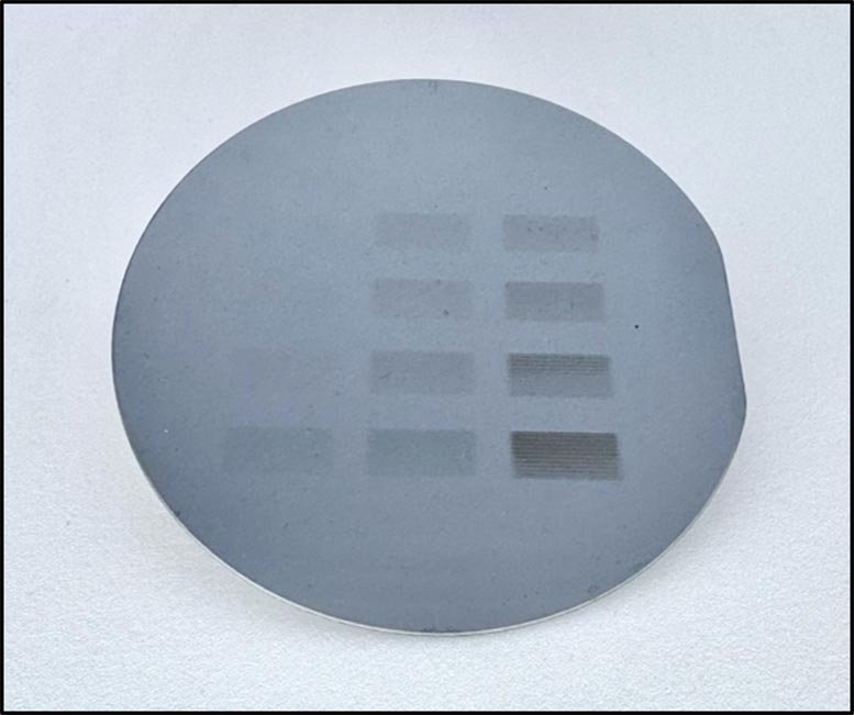
Micropuces are flat pieces of silicon with printed circuits that perform basic functions. During production, manufacturers envelop silicon slices with a material sensitive to radiation to create a very fine coating called “resistance”. When a radiation beam is pointed out on resistance, it triggers a chemical reaction that burns the details in the edge, drawing patterns and circuits.
However, the more powerful radiation beams that are necessary to cut more and more the smallest details on the fleas do not interact strongly enough with traditional resistances.
Push up the current limits
Previously, researchers from the TsapatSis and Fairbrother Research Group laboratory of Johns Hopkins have found that resisting a new class of metal organisms can adapt to this more powerful process of radiation, called “beyond the extreme ultraviolet radiation” (B-EUV), which has the potential to make the details smaller than the standard size of 10 nanometers. Metals like zinc absorb B-EUV light and generate electrons that cause chemical transformations necessary to print circuits models on an organic material called imidazole.
This research marks one of the first times that scientists have been able to deposit these metal-organic resistances based on imidazole from the solution to the scale of silicon-wafer, controlling their thickness with nanometric precision. To develop the chemistry necessary to cover the silicon slice with metal-organic materials, the team combined experiences and models from Johns Hopkins University, the University of Sciences and Technologies in eastern China and the Federal Polytechnic School of Lausanne, University of Soochow, Brookhaven National Laboratory and Lawrence Berkeley National Laboratory. The new methodology, which they call the deposit of chemical fluid (CLD), can be designed with precision and allows researchers to quickly explore various combinations of metals and imidazoles.
“By playing with the two components (metal and imidazole), you can change the effectiveness of the absorption of light and chemistry of the following reactions.” What is exciting is that there are at least 10 different metals which can be used for this chemistry and hundreds of organics. “
At the end of new generation manufacturing
The researchers began to experiment with different combinations to create agreements specifically for B-EUV influence, which, according to them, will probably be used in manufacturing over the next 10 years.
“Because different wavelengths have different interactions with different elements, a metal which is a loser in a wavelength can be a winner with the other,” said Tsapatsis. “Zinc is not very good for extreme ultraviolet radiation, but it is one of the best for the B-EUV.”
Reference: “Spin-on deposit of imbasy amorphic frame movies imidazolate for lithography applications” by Yurun Miao, Shunyi Zheng, Kayley E. Waltz, Mueed Ahmad, Xinpei Zhou, Yegui Zhou, Hunting Wang, J. Anibal BoscoMenik, Qi Liu, Kumar Varsko, Liwei Zhuang and Michael Tsapatsis, September 11, 2025, Chemical genius of nature.
DOI: 10.1038 / S44286-025-00273-Z
The authors include Yurun Miao, Kayley Waltz and Xinpei Zhou of Johns Hopkins University; Liwei Zhuang, Shunyi Zheng, Yegui Zhou and Hunting Wang from the University of Eastern Sciences and Technologies; MUEED AHMAD and J. Anibal BOSCOBOINIK from the Brookhaven National Laboratory; Qi liu from SOOOCHOW University; Kumar Varoon Agrawal of Federal Polytechnic School of Lausanne; and Oleg Kostko of Lawrence Berkeley National Laboratory.
Never miss a breakthrough: join the Scitechdaily newsletter.
:max_bytes(150000):strip_icc()/Health-GettyImages-1384262057-f6600cac1add4a859131046fb92bcec2.jpg?w=390&resize=390,220&ssl=1 "Can stress really cause hemorrhoids?")


